Date of publication: 10/12/16 Very often people dream of a window. This symbol...


By this time, some components (resistors, capacitors) had already been developed and mastered, which were used in the manufacture of GIS and SMEs. However, TMP tightened the requirements for resistance to climatic factors, since chip resistors and capacitors for GIS and SMEs were manufactured in an unprotected design for use inside GIS cases.
Currently, an extensive range of components for TMP has been developed, including resistors, capacitors (including variable ones), inductors, microtransformers, relays, quartz resonators, diodes, transistors, microcircuits, microswitches, etc. These components have several types of housings: leadless with tinned ends, with shortened gull wing or J-shaped leads, cylindrical housings with metallized ends. Let's take a closer look at these cases.
Chip body - leadless rectangular package for simple passive components such as resistors, jumpers and capacitors (Figure 2.1).
Figure 2.1 - Housings of simple chip components
Chip resistors and chip capacitors are manufactured using group technology on large-sized substrates (usually 60x48 mm), then after scribing the substrate is broken into separate parts (the English word chip means fragment). After breaking, a multilayer metallization (thick film conductor - nickel barrier layer - solder layer) is applied to the ends of the chip component on three or five sides for each end (the latter option is used for highly reliable components). In the manufacture of chip resistors, thick film technology is usually used. A typical design of a thick film chip resistor is shown in Figure 2.2. The resistor consists of a ceramic base (A1 2 O 3 substrate), a resistive layer (ruthenium oxide), an internal contact layer (palladium-silver), an intermediate nickel barrier layer, and an external contact layer (tin-lead alloy). The resistor body is protected by a borosilicate glass coating with an indelible code marking of the value.
Figure 2.2 - Design of a thick film chip resistor
The marking of resistors consists of three digits for simple and four digits for high-precision resistors, with the last digit indicating the number of zeros that must be added to the right of the Ohm value. For example: 160-16 Ohm, 472-4.7 kOhm, 112-1.1 kOhm, 106 - 10 MOhm, 2741 - 2.74 kOhm. The marking of low-resistance resistors contains the letter “R”, for example, 4R7 - 4.7 Ohms, 54R9 - 54.9 Ohms.
Chip jumpers, the resistance of which should not exceed 0.05 Ohm, are marked 000.
Capacitors are usually marked on the packaging container. Symbol for capacity: the first two digits indicate the nominal value in picofarads, the third digit indicates the number of zeros added to the right. For example: 105 - 1 µF, 153 - 0.015 µF.
Electrolytic capacitors that have a sufficiently large surface area may contain a coded designation of the operating voltage and capacitance value. Several encoding options are possible:
a) the code contains two or three characters (letters or numbers). The letters indicate voltage and capacitance, and the number indicates the multiplier

The letters may be preceded by a number indicating the range of operating voltages:
b) the code contains four characters (letters and numbers) indicating the rated capacity and operating voltage. The first letter indicates the voltage, the next two digits indicate the capacitance in pF, and the last digit represents the number of zeros. For example: E475 is a capacitor with a capacity of 4.7 μF with an operating voltage of up to 25 V. Sometimes the capacitance can be indicated using the letter c: E4ts7 is the designation of a capacitor corresponding to the above example.
In general, a chip component can be characterized by dimensions L (length), B (width), H (height), D or / (pad width) as shown in Figure 2.3. The sizes of chip resistors depend on the power dissipation, and the sizes of chip capacitors depend on the nominal capacitance and operating voltage.
The shape and dimensions of the housings are standardized by international and national standards (IEC115, IEC384). These standards use a designation system for the design of the KMP in the form of two pairs of numbers that characterize the length and width of the housing in hundredths of an inch (sizes from 0101 (0.25x0.25 mm) to 2225 (5.7x6.3 mm). Comparative sizes of some The sizes of resistors compared to a match head against the background of a 1.27 mm grid are shown in Figure 2.4.
Some companies give the designation of the standard size of the case in mm: 1005 - (1.0x0.5) mm, which corresponds to the above designation of the case 0402; 3216 - (3.2x1.6) mm - corresponds to the designation 1206.
Domestic industry produces chip resistors for general use R1-12, precision resistors R1-16, sets of resistors HP1-29, chip jumpers P1-23. Jumper chips are used to provide transitions across wires during topology design. They are produced with overall dimensions of 3.2x1.6x0.6 mm (1206) and have a resistance of no more than 0.05 Ohm.
Chip capacitors for surface mounting are represented by multilayer ceramic ones (K10-9M, K10-17-4v, K10-42, K10-43, K10-47, K10-50v, K10-56, K10-57, K10-60v, K10 -69, K10-73-6v), tantalum oxide semiconductor (K53-25, K53-36, K53-37) and aluminum oxide semiconductor K53-40.
MELF housing(Metal Electrode Face Bonded) - a cylindrical body with built-in electrodes in the form of metallized ends (Figure 2.5). Designed for diodes, resistors, capacitors, inductors. The case diameter ranges from 1.25 mm to 2.2 mm, length - from 2 to 5.9 mm.
The MELF housing has a low cost, but its installation is difficult. It became widespread in Japan at the beginning of the development of TMP. Examples of domestic components in such packages are resistors Pl-11, P1-30.
Small Diode SOD Package(Small Outline Diode) - a plastic case with two gull-wing terminals (Figure 2.6). Designed for diodes, LEDs, varicaps. The most common is the SOD-80 housing, the domestic analogue of which is the KD-34 housing in accordance with GOST 18472-88.


Figure 2.5 - MELF type housing Figure 2.6 - SOD type housing
Small SOT Transistor Package(Small Outline Transistor) has from 3 to 6 outputs (Figure 2.7).

Figure 2.7 - SOT type enclosures
The case has a plastic shell and shortened gull-wing type leads. In addition to transistors, diodes, varicaps, and amplifiers can be mounted in it. It is the first surface mount package whose development program was implemented by Siemens more than 25 years ago. The most common SOT-23 package has dimensions of 2.9x1.3x1.1 mm.
Further developments of this type of housing are SOT-89, SOT-143, S-mini, SS-mini. Subsequent developments are characterized by a reduction in the distance between the pins to 0.65 -0.5 mm, which made it possible to reduce the dimensions of the case to 1.6x1.6x0.75 mm. Domestic cases of this type are represented by cases KT-46 (SOT-23), KT-47 (SOT-89), KT-48 (SOT-143). The main geometric dimensions of the housings are shown in Figure 2.8.
SOT-23 (KT-46)
 SOT-89 (KT-47)

Figure 2.8 - Overall dimensions of SOT type enclosures
Small-sized packages for microcircuits can be combined into several groups depending on the shape of the leads (gull-wing, J-shaped lead), their location on two or four sides of the housing, and the material of the housing (plastic or ceramic):
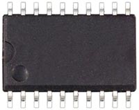
- housing typeSOIC (Small Outline Integrated Circuit) u SOP (Small Outline Packages) with double-sided pinouts in the shape of a gull wing (Figure 2.9a, 2.9.6). The pin spacing for this type of case is 1.27 mm, the number of pins is from 6 to 42. A further development of cases of this type was the creation of the case SSOIC (Shrink Small Outline Integrated Circuit) with the distance between pins reduced to 0.635 mm with a maximum number of 64 (Figure 2.9c) and housing TSOP (Thin Small Outline Packages) with the body height reduced to 1.27 mm (Figure 2.8d) and the distance between the pins reduced to 0.3 - 0.4 mm;
- housing typeSOJ (Small Outline with “J” leads) with a double-sided arrangement of J-shaped leads, bent under the housing (Figure 2.10). The pitch of the pins is 1.27 mm, their total number is from 14 to 28.

Figure 2.9 - Varieties of microcircuit packages with double-sided pinouts in the shape of a gull wing: a-SOIC type package; b-body type SOP; c - SSOIC type housing; g - TSOP type housing

Figure 2.10 - Microcircuit case with J-shaped leads: a - general view of the case; b - terminal design
- housing typeQFP (Quad Flat Pack) and SQFP (Shrink Quad Flat Pack), having leads in the shape of a “gull wing”, evenly distributed on four sides (Figure 2.11 a). There is also a type of rectangular-shaped case - SQFP-R (Figure 2.11 b). The pitch of the pins is quite small - only 0.3 - 0.5 mm, which allows you to create cases with a total number of pins up to 440;

Figure 2.11 - Varieties of microcircuit packages with four-sided pinouts in the shape of a gull wing: a - QFP and SQFP package; b-case type SQFP-R
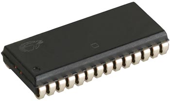
- housing typePLCC (Plastic Leaded Chip Carrier) - a square plastic crystal carrier with J-leads (Figure 2.12a) and typePLCC- R (Plastic Leaded Chip Carrier Rectangular) - a rectangular plastic crystal carrier with J-leads (Figure 2.126). Cases of this type have a significant pin spacing by modern standards - 1.27 mm and, therefore, large geometric dimensions. The number of pins for a square case is from 20 to 124, for a rectangular case - from 18 to 32;

Figure 2.12 - IC case with J-shaped leads
and four-sided pin arrangement:
a-square PLCC; b-rectangular PLCC-R
- LCCC housings(Leadless Ceramic Chip Carrier) - leadless ceramic crystal carrier (Figure 2.13). On the side surfaces of such a case there are special metallized recesses located in increments of 1.27 mm, which serve to form an electrical connection with the contact pads of the board when soldering the assembly with dosed solder.

Figure 2.13- LCCC housing
The domestic analogue of SOIC type enclosures are subtype 43 enclosures in accordance with GOST 17467-88. Dimensional drawings and dimensions of these housings are shown in Figure 2.14 and Table 2.1.

Figure 2.14 - Overall dimensions of subtype 43 housings
Table 2.1 - Overall dimensions of 43 V subtype housings millimeters
|
Size code |
Number of pins |
||||
The domestic analogue of QFP type housings are subtype 44 housings in accordance with GOST 17467-88. Dimensional drawings and dimensions of these housings are shown in Figure 2.15 and Table 2.2.
The global electronics industry produces about 90% of all TMP ICs in plastic cases and only 10% in ceramic ones. Ceramic cases have significantly higher performance indicators. Thus, the operating temperature range of microcircuits in ceramic cases is from -55 to +125°C, and in plastic cases - from -10 to +85°C. However, ceramic cases have a large mass and cost, so they are used, as a rule, in the most critical cases.

Figure 2.15 - Overall dimensions of subtype 44 housings
Table 2.2 - Overall dimensions of subtype 44 housings
|
Size code |
Number of pins |
|||||
Non-standard housings for irregularly shaped components such as switches, fuses, inductors, electrolytic capacitors, and variable resistors are shown in Figure 2.16.

Figure 2.16 - Non-standard housings for ILC
The domestic industry produces tuning resistors in the TMP version of the following types: RP1-75, RP1-82, RP1-83, RP1-98. Resistors have a resistance range from 10 Ohms to 3.3 MOhms, allowing power dissipation of 0.25 W. Overall dimensions do not exceed 4.5x4.5x3.5 mm.
An integrated circuit package (IC) is a sealed structure designed to protect the integrated circuit chip from external influences and to provide electrical connections to external circuits. The length of the microcircuit body depends on the number of pins. Let's look at some types of housings that are most often used by radio amateurs.
DIP (Dual In-line Package)- type of housing for microcircuits, microassemblies and some other electronic components for installation in holes of a printed circuit board, is the most common type of housing. It has a rectangular shape with two rows of pins on the long sides. Can be made of plastic or ceramic. The housing designation indicates the number of pins. Various semiconductor or passive components can be produced in a DIP package - microcircuits, diode assemblies, TTL logic, generators, amplifiers, op-amps and others... Components in DIP packages usually have from 4 to 40 pins, perhaps there are more. Most components have a pin pitch of 2.54 millimeters and a row spacing of 7.62 or 15.24 millimeters.
One type of DIP package is the QDIP package. This package has 12 pins and usually has petals for attaching the microcircuit to a radiator, remember the K174UN7 microcircuit.

A type of DIP is PDIP – (PlasticDualIn-linepackage)– the housing is rectangular in shape and equipped with leads intended primarily for mounting into holes. There are two types of housing: narrow, with a pin spacing of 7.62 mm, and wide, with a pin spacing of 15.24 mm. There are no differences between DIP and PDIP in terms of housing; PDIP is usually made of plastic, CDIP is made of ceramic. If the microcircuit has many pins, for example 28 or more, then the case can be wide.

SIP (Single In-line Package)– a flat housing for vertical mounting into the holes of a printed circuit board, with one row of pins on the long side. Usually the designation also indicates the number of pins. The numbering of the pins of these types of microcircuits starts on the left when looking at the markings from the front.

TO92 – a common type of package for low-power transistors and other semiconductor devices with two or three terminals, including microcircuits, such as integrated voltage regulators. In the USSR, this type of hull was designated KT-26.

TO220- type of housing for transistors, rectifiers, integrated voltage stabilizers and other low and medium power semiconductor devices. The numbering of pins for different elements may differ, transistors have one designation, voltage stabilizers have another...

PENTAWATT– Contains 5 pins; such housings are used, for example, for low-frequency amplifiers (TDA2030, 2050...) or voltage stabilizers.

DPAK- (TO-252, KT-89) housing for housing semiconductor devices. The D2PAK is similar to the DPAK body, but larger; Basically equivalent to TO220 for SMD mounting, they come in three, five, six, seven or eight pins.

SO (Small Outline) small plastic case. The housing has a rectangular shape and is equipped with terminals intended for surface mounting. There are two types of case: narrow, with a case width of 3.9 mm (0.15 inches) and wide, with a case width of 7.5 mm (0.3 inches).
SOIC (Small-Outline Integrated Circuit) - designed for surface mounting, essentially the same as SO. It has the shape of a rectangle with two rows of pins on the long sides. As a rule, the numbering of pins of identical microcircuits in DIP and SOIC packages is the same. In addition to the abbreviation SOIC, the letters SO can be used to designate enclosures of this type, as well as SOP (Small-Outline Package) and the number of pins. Such enclosures can have different widths. Usually designated as SOxx-150, SOxx-208 and SOxx-300 or written SOIC-xx and indicate which drawing it corresponds to. This type of enclosure is similar to QSOP.

There is also a version of the housing with pins bent under the housing (in the shape of the letter J). This type of housing is designated as SOJ (Small-Outline J-leaded).
QFP (Quad Flat Package) - a family of microcircuit packages that have planar pins located on all four sides. The shape of the base of the microcircuit is rectangular, and often a square is used. Packages usually differ only in the number of pins, pitch, dimensions and materials used. BQFP It is distinguished by base extensions at the corners of the microcircuit, designed to protect the leads from mechanical damage before sealing.

This family includes housings TQFP (Thin QFP) QFP LQFP (Low-profile QFP). Microcircuits in such packages are intended for surface mounting only; installation in a connector or mounting in holes is not standardly provided, although transition switching devices exist. The number of QFP chip pins usually does not exceed 200, with pitches from 0.4 to 1.0 mm. The overall dimensions of the housings and the distance between the terminals can be viewed.

QFN (Quad-flat no-leads)– in such cases, as well as in SOJ cases, the leads are bent under the case. Overall dimensions and distance between pins of QFN packages can be viewed. This case is similar to the type of cases MLF, their outputs are located along the perimeter and below.

TSOP (Thin Small-Outline Package)– these cases are very thin, low-profile, and are a type of SOP chips. They are used in DRAM memory modules and for flash memory chips, especially for packaging low-voltage microcircuits due to their small volume and large number of pins (contacts). In more modern memory modules, such packages are no longer used; they have been replaced by BGA-type packages. There are usually two types of cases, they are shown in the photo below.

PLCC (Plastic Leaded Chip Carrier) and CLCC (Ceramic Leaded Chip Carrier)- are a square housing with contacts located along the edges, designed for installation in a special panel (often called a “crib”). Currently, flash memory chips in PLCC packages are widely used as BIOS chips on motherboards. The overall dimensions of the housings and the distance between the terminals can be viewed.

ZIP (Zigzag-In-line Package)- flat housing for vertical mounting into printed circuit board holes with pins arranged in a zigzag pattern. There are ZIP12, ZIP16, ZIP17, ZIP19, ZIP20, ZIP24, ZIP40 numbers indicate the number of pins and the type of housing; in addition, they differ in the dimensions of the housings, as well as the distance between the pins. The overall dimensions of the housings and the distance between the terminals can be viewed.
The modern radio amateur now has access to not only ordinary components with leads, but also such small, dark parts that you can’t understand what’s written on them. They are called "SMD". In Russian this means "surface mount components". Their main advantage is that they allow the industry to assemble boards using robots that quickly place SMD components in their places on the printed circuit boards, and then mass bake them to produce assembled printed circuit boards. The human share remains with those operations that the robot cannot perform. Not yet.
The use of chip components in amateur radio practice is also possible, even necessary, as it allows you to reduce the weight, size and cost of the finished product. Moreover, you practically won’t have to drill.
For those who first encountered SMD components, confusion is natural. How to understand their diversity: where is the resistor, and where is the capacitor or transistor, what sizes do they come in, what types of SMD parts are there? You will find answers to all these questions below. Read it, it will come in handy!
Quite conventionally, all surface-mount components can be divided into groups according to the number of pins and housing size:
| pins/size | Very very small | Very small | Little ones | Average |
| 2 outputs | SOD962 (DSN0603-2) , WLCSP2*, SOD882 (DFN1106-2) , SOD882D (DFN1106D-2) , SOD523, SOD1608 (DFN1608D-2) | SOD323, SOD328 | SOD123F, SOD123W | SOD128 |
| 3 pins | SOT883B (DFN1006B-3) , SOT883, SOT663, SOT416 | SOT323, SOT1061 (DFN2020-3) | SOT23 | SOT89, DPAK (TO-252), D2PAK (TO-263), D3PAK (TO-268) |
| 4-5 pins | WLCSP4*, SOT1194, WLCSP5*, SOT665 | SOT353 | SOT143B, SOT753 | SOT223, POWER-SO8 |
| 6-8 pins | SOT1202, SOT891, SOT886, SOT666, WLCSP6* | SOT363, SOT1220 (DFN2020MD-6), SOT1118 (DFN2020-6) | SOT457, SOT505 | SOT873-1 (DFN3333-8), SOT96 |
| > 8 pins | WLCSP9*, SOT1157 (DFN17-12-8) , SOT983 (DFN1714U-8) | WLCSP16*, SOT1178 (DFN2110-9) , WLCSP24* | SOT1176 (DFN2510A-10) , SOT1158 (DFN2512-12) , SOT1156 (DFN2521-12) | SOT552, SOT617 (DFN5050-32), SOT510 |
Of course, not all packages are listed in the table, since the real industry produces components in new packages faster than the standardization bodies can keep up with them.
The housings of SMD components can be either with or without leads. If there are no leads, then there are contact pads or small balls of solder (BGA) on the case. Also, depending on the manufacturer, parts may differ in markings and dimensions. For example, capacitors may vary in height.

Most SMD component housings are designed for installation using special equipment that radio amateurs do not have and are unlikely to ever have. This is due to the technology of soldering such components. Of course, with a certain persistence and fanaticism, you can solder at home.
Types of SMD housings by name
| Name | Decoding | number of pins |
| SOT | small outline transistor | 3 |
| SOD | small outline diode | 2 |
| SOIC | small outline integrated circuit | >4, in two lines on the sides |
| TSOP | thin outline package (thin SOIC) | >4, in two lines on the sides |
| SSOP | seated SOIC | >4, in two lines on the sides |
| TSSOP | thin seated SOIC | >4, in two lines on the sides |
| QSOP | Quarter size SOIC | >4, in two lines on the sides |
| VSOP | Even smaller QSOPs | >4, in two lines on the sides |
| PLCC | IC in a plastic case with leads bent to form a letter-shaped case J | >4, in four lines on the sides |
| CLCC | IC in a ceramic package with leads bent to form a letter-shaped package J | >4, in four lines on the sides |
| QFP | square flat case | >4, in four lines on the sides |
| LQFP | low profile QFP | >4, in four lines on the sides |
| PQFP | plastic QFP | >4, in four lines on the sides |
| CQFP | ceramic QFP | >4, in four lines on the sides |
| TQFP | thinner than QFP | >4, in four lines on the sides |
| PQFN | power QFP without leads with a pad for a radiator | >4, in four lines on the sides |
| BGA | Ball grid array. Array of balls instead of pins | pin array |
| LFBGA | low profile FBGA | pin array |
| C.G.A. | housing with input and output terminals made of refractory solder | pin array |
| CCGA | CGA in ceramic case | pin array |
| μBGA | micro BGA | pin array |
| FCBGA | Flip-chip ball grid array. Man array of balls on a substrate to which a crystal with a heat sink is soldered | pin array |
| LLP | leadless housing |
From this whole zoo of chip components that can be used for amateur purposes: chip resistors, chip capacitors, chip inductors, chip diodes and transistors, LEDs, zener diodes, some microcircuits in SOIC packages. Capacitors usually look like simple parallelipipeds or small barrels. The barrels are electrolytic, and the parallelepipeds will most likely be tantalum or ceramic capacitors.

Chip components of the same denomination may have different dimensions. The dimensions of an SMD component are determined by its “standard size”. For example, chip resistors have standard sizes from “0201” to “2512”. These four digits encode the width and length of the chip resistor in inches. In the tables below you can see the standard sizes in millimeters.

| Rectangular chip resistors and ceramic capacitors | |||||
| Standard size | L, mm (inch) | W, mm (inch) | H, mm (inch) | A, mm | W |
| 0201 | 0.6 (0.02) | 0.3 (0.01) | 0.23 (0.01) | 0.13 | 1/20 |
| 0402 | 1.0 (0.04) | 0.5 (0.01) | 0.35 (0.014) | 0.25 | 1/16 |
| 0603 | 1.6 (0.06) | 0.8 (0.03) | 0.45 (0.018) | 0.3 | 1/10 |
| 0805 | 2.0 (0.08) | 1.2 (0.05) | 0.4 (0.018) | 0.4 | 1/8 |
| 1206 | 3.2 (0.12) | 1.6 (0.06) | 0.5 (0.022) | 0.5 | 1/4 |
| 1210 | 5.0 (0.12) | 2.5 (0.10) | 0.55 (0.022) | 0.5 | 1/2 |
| 1218 | 5.0 (0.12) | 2.5 (0.18) | 0.55 (0.022) | 0.5 | 1 |
| 2010 | 5.0 (0.20) | 2.5 (0.10) | 0.55 (0.024) | 0.5 | 3/4 |
| 2512 | 6.35 (0.25) | 3.2 (0.12) | 0.55 (0.024) | 0.5 | 1 |
| Cylindrical chip resistors and diodes | |||||
| Standard size | Ø, mm (inch) | L, mm (inch) | W | ||
| 0102 | 1.1 (0.01) | 2.2 (0.02) | 1/4 | ||
| 0204 | 1.4 (0.02) | 3.6 (0.04) | 1/2 | ||
| 0207 | 2.2 (0.02) | 5.8 (0.07) | 1 | ||
Ceramic chip capacitors are the same size as chip resistors, but tantalum chip capacitors have their own size system:

| Tantalum capacitors | |||||
| Standard size | L, mm (inch) | W, mm (inch) | T, mm (inch) | B, mm | A, mm |
| A | 3.2 (0.126) | 1.6 (0.063) | 1.6 (0.063) | 1.2 | 0.8 |
| B | 3.5 (0.138) | 2.8 (0.110) | 1.9 (0.075) | 2.2 | 0.8 |
| C | 6.0 (0.236) | 3.2 (0.126) | 2.5 (0.098) | 2.2 | 1.3 |
| D | 7.3 (0.287) | 4.3 (0.170) | 2.8 (0.110) | 2.4 | 1.3 |
| E | 7.3 (0.287) | 4.3 (0.170) | 4.0 (0.158) | 2.4 | 1.2 |
Inductors are found in many types of housings, but the housings are subject to the same size law. This makes automatic installation easier. And it makes it easier for us, radio amateurs, to navigate.
All kinds of coils, chokes and transformers are called “winding products”. Usually we wind them ourselves, but sometimes you can buy ready-made products. Moreover, if SMD options are required, which come with many bonuses: magnetic shielding of the housing, compactness, closed or open housing, high quality factor, electromagnetic shielding, wide range of operating temperatures.

It is better to select the required coil according to catalogs and the required standard size. Standard sizes, as for chip resistors, are specified using a four-number code (0805). In this case, “08” indicates the length, and “05” the width in inches. The actual size of such an SMD component will be 0.08x0.05 inches.
Diodes can be either in cylindrical cases or in cases in the form of small parallelipipeds. Cylindrical diode packages are most often represented by MiniMELF (SOD80 / DO213AA / LL34) or MELF (DO213AB / LL41) packages. Their standard sizes are set in the same way as for coils, resistors, and capacitors.

| Diodes, Zener diodes, capacitors, resistors | |||||
| Type of shell | L* (mm) | D* (mm) | F* (mm) | S* (mm) | Note |
| DO-213AA (SOD80) | 3.5 | 1.65 | 048 | 0.03 | JEDEC |
| DO-213AB (MELF) | 5.0 | 2.52 | 0.48 | 0.03 | JEDEC |
| DO-213AC | 3.45 | 1.4 | 0.42 | - | JEDEC |
| ERD03LL | 1.6 | 1.0 | 0.2 | 0.05 | PANASONIC |
| ER021L | 2.0 | 1.25 | 0.3 | 0.07 | PANASONIC |
| ERSM | 5.9 | 2.2 | 0.6 | 0.15 | PANASONIC, GOST R1-11 |
| MELF | 5.0 | 2.5 | 0.5 | 0.1 | CENTS |
| SOD80 (miniMELF) | 3.5 | 1.6 | 0.3 | 0.075 | PHILIPS |
| SOD80C | 3.6 | 1.52 | 0.3 | 0.075 | PHILIPS |
| SOD87 | 3.5 | 2.05 | 0.3 | 0.075 | PHILIPS |
Surface mount transistors can also be of low, medium and high power. They also have matching housings. Transistor cases can be divided into two groups: SOT, DPAK.

I would like to draw your attention to the fact that such packages may also contain assemblies of several components, not just transistors. For example, diode assemblies.
Sometimes it seems to me that the marking of modern electronic components has turned into a whole science, similar to history or archeology, since in order to figure out which component is installed on the board, sometimes you have to conduct a whole analysis of the elements surrounding it. In this regard, the Soviet output components, on which the denomination and model were written in text, were simply a dream for an amateur, since there was no need to rummage through piles of reference books to figure out what these parts were.
The reason lies in the automation of the assembly process. SMD components are installed by robots, in which special reels are installed (similar to the reels with magnetic tapes) in which chip components are located. The robot doesn’t care what’s in the bag or whether the parts are marked. Humans need labeling.
At home, chip components can only be soldered up to a certain size; size 0805 is considered more or less comfortable for manual installation. Smaller components are soldered using a stove. At the same time, for high-quality soldering at home, a whole range of measures should be observed.
Modern surface mounting technology provides the following requirements for electronic
nal components:
Minimum weight and dimensions, flatness, low profile of leads, low cost, ensuring standardization;
Suitability for automated installation, the ability to use existing soldering methods;
High temperature resistance under conditions of prolonged thermal stress during the soldering process
possibility of modern packaging.
Currently, the EC market has a large
selection of elements in various housings for surface-
installation. Moreover, the development of cases for
The EC has approached a stage where its role is
becomes as important as the development of the components themselves
nentov. The main components for surface-
th installation are large (BIS) and extra-large
(VLSI) integrated circuits (ICs) and semiconductor
high-quality devices in small-sized housings. Exists
large selection of housings for surface
installation It should be noted that the IC die dimensions
continue to increase, and the sizes of elements in
it – are decreasing, so specialists occupy
problems with assembling components, we were faced with
double problem. Firstly, it is necessary to collect
physically large crystal, high density
elements in which requires an increase in the number of con
tact pads for connecting it with internal
body terminals. Secondly, the increase in size and
packing densities of elements in LSI crystals and
VLSI requires an increase in the number of pins in packages,
in which they are mounted, which can lead to
increase in their size, weight, deterioration of electrical
technical characteristics and speed of microdevices
ditch
Therefore, the LSI and VLSI packaging technology is
dynamic, rapidly developing area of micro-
electronics, with the main trend being
the desire to minimize the volume of the body with -
simultaneous increase in the number of pins with a decrease in the distance between them.
Housings are classified depending on
from design features and geometric
sizes. Classification of housings for surfaces
detailed installation is shown in Figure 2.40. In accordance with
This classification in table 2.13 shows the main
detailed data on the most common and promising types of enclosures.
It should be noted that some
ry manufacturers in the reference data as the main
new, the company designation of the case is given, and
in the comments they provide information about the compliance of the brand name
designations generally accepted. Besides,
often before generally accepted corporate designations
owls put a letter identifying the material from which
the case is made: P - plastic, C - ceramics, M - me-
tall ceramics.
Figure 2.40 - Classification of microcircuit packages intended for
surface mount
Housings with leads around the perimeter are included in the
families SOP, SOJ, QFJ, QFP, DIP. The most
extensive SOP housings (number of pins from 8 to 100)
and QFP (number of pins from 20 to 304). In buildings
with a large number of pins they produce digital micro-
schemes of medium and high degree of integration, and
packages with a small number of pins - digital
microcircuits of small and medium degree of integration,
analog microcircuits, diodes and transistors.
TCP-designed microcircuits have tape
terminals made of thin copper or aluminum foil on
polymer film attached to the solder crystal
Coy or ultrasonic welding. After installation on
The chip board must be sealed in
ve boards. They are supplied on a carrier tape and
well suited for automated control
monitoring parameters and installation. This type of chip
used in inexpensive, non-repairable -
equipment with large output volumes.
For high and ultra high grade chips
integration has become widespread in recent years
proliferation of BGA packages, since they are
relatively inexpensive and with large quantities you-
waters take up little space on the board. According to technical
BGA nology unpackaged crystals (single or non-
how much) mounted on the surface of a printed micro-
roplaty and sealed with a polymer compound.
Microcircuits in BGA packages are soldered onto boards using pins made in the form of an array of solder balls on the contact pads of the microboard. Further development of BGA package technology led to the creation of CSP-type packages, in which there is no printed circuit board, and the ball leads are placed directly on the contact pads in the upper layer of the crystal metallization. After forming the ball leads, the crystal is filled with a thin layer of plastic and mounted on a printed circuit board in the same way as a BGA package. If necessary, a heat sink is installed on the upper side of the microcircuit. With the efficient use of board area, this technology is practically not inferior to flip-chip technology (mounting inverted, unpackaged crystals on a board and sealing them with a polymer compound as part of the board). The main obstacle to the mass production of microcircuits in CSP packages and the widespread use of flip-chip technology is the lack of reliable and reliable
an expensive way to reduce voltage in the system
crystal-PCB arising due to spills
The temperature coefficient of expansion of a semiconductor crystal (2×10 -6 /°C), copper (16.6×10 -6 /°C)
and dielectric type FR-4 ((15...19)×10 -6 /°С), from which
they make printed circuit boards.
Therefore, the main efforts
developers are aimed at increasing the reliability
of such microcircuits by creating between the crystal
and a low-cost transition structure board that quenches
temperature stresses.
Table 2.13 - Surface mount chip packages
| Frame | Short description | Lead pitch, mm | Appearance of the case | |
| Type | Full title | |||
| 1. Cases for microcircuits of low, medium and high degrees of integration 1.1. With leads along two sides of the case 1.1.1. With standard pin spacing | ||||
| SO, SOP, SOL, SOIC | Small Outline Package, Small Outline Integrated Circuit | Gullwing or L-shaped terminals | 1.27 | |
| SOJ | Small Outline J-Lead Package | J-shaped terminals | 1.27 | |
| TSOP option 2 | Thin Small Outline Package | The case has a reduced height above the board (no more than 1.27 mm), the pins are located along the long side of the case | 1.27 | |
| 1.1.2. With reduced pin spacing | ||||
| TSOP option 1 | Thin Small Outline Package | Case with reduced height above the board (no more than 1.27 mm), pins are located along the short side of the case | 0.5 | |
| SSOP, SSOL | Shrink Small Outline Package | Koppyc SOP with reduced pin pitch | 1.00 0. 80 0.65 0.50 | |
| TSSOP | Thin Shrink Small Outline Package | SSOP case with reduced height above the board (no more than 1.27 mm). Standardized by EIAJ, JEDEC | 0.65 0.50 | |
| TVSOP | Thin Very Small Outline Package | Miniature SOP housing | 0,10 | |
| uSOIC | microSOIC | Miniature SOIC package | 0.65 | |
| 1.2. With leads along four sides of the housing 1.2.1. With standard case sizes | ||||
| QFP | Quad Flat Package | Gullwing pins along four sides of the body | 1.00 0.80 0. 65 | |
| PLCC | Plastic Leaded Chip Carrier | Crystal carrier with leads in the form of the letter G. Standardized by EIAJ, JEDEC | 1.27 0.636 |
Continuation of Table 2.13 - Surface Mount IC Packages
| Frame | Short description | Lead pitch, mm | Appearance of the case | |
| Type | Full title | |||
| 1.2.2. With reduced body dimensions | ||||
| LQFP, NQFP | Low Profile (Thin) Quad Flat Package | OFP case with reduced height above the board (no more than 1.27 mm) | 0.80 0.65 | |
| MQFP | Metric Thin Quad Flat Package | QFP package with metric pin spacing and reduced board height | 0.60 | |
| FQFP | Fine Pitch Quad Flat Package | OFP package with fine pin pitch. Standardized by EIAJ | 0.40 | |
| 1.3. With pin matrix on the bottom surface of the housing | ||||
| BGA | Ball Grid Array | A microcircuit or multi-chip module on a two-layer printed circuit board, equipped with an array of ball pins | 1.27, 1.00 | |
| C.P.S. | Chip Scale Package | A case with dimensions slightly larger than the dimensions of the crystal. Equipped with an array of ball leads | 1.00, 0.50 | |
| 2. Housing a for transistors and microcircuits of low degree of integration 2.1. Low power dissipation | ||||
| SOT-23 | Small Outline Transistor | For diodes, transistors, microcircuits with a small number of pins. SOT-23 is also available in a version with five (SOT-5, SOT-23-5) or six (SOT-6, S0T-23-6) pins | 0.95 | |
| SOT-143 | 1.90 | |||
| SOT-323 | 0.65 | |||
| SOT-363 | 0.65 | |||
| 2.2. With average power dissipation | ||||
| SOT-223 | Small Outline Transistor | For transistors and microcircuits with a small number of pins (DC/DC converters, voltage stabilizers) | 1.95 | |
| DPAC | D-package | 4.80 | ||
| 2.3. With high power dissipation | ||||
| D 2 PAC | D-package | For transistors and microcircuits with increased power dissipation, high supply voltage Typically, these are devices with pulse currents up to 100 A | 2.54/ 5.08 | |
| D 3 PAC | D-package | 10.9 |
For microcircuits with a regular structure,
low power consumption and small quantity
number of pins (typical representatives of such microcircuits
- memory chips) began to develop technical
nology for the manufacture of multi-level (“shelf-shelves”)
nyh") 3DM modules. According to one of the options
of this technology, each level is performed analogously
gically to the BGA chip, the crystal is installed -
using the flip-chip method and is filled with a layer of polymer com-
pound. Microboards of different levels are then assembled
in a column, ball leads are soldered to create
of vertical connecting conductors, boards
The columns are fastened with a polymer compound. Semi-
The finished module is mounted on the board using -
ball leads.
The SOT family cases were originally designed
worked for transistors and had three outputs (using
connecting SOT-363, which had 6 pins). One-
subsequently, manufacturers began to use these
housings for microcircuits, if necessary, enlarge
changing the number of pins while maintaining the same dimensions
ritov. In particular, microcircuits are produced in -
packages SOT-23 with five pins and D2PAK with four.
From the designer's point of view, the variety of types
The size of the packages slightly complicates the process of developing printed circuit boards if their dimensions are specified in one measuring system. And vice versa, the development process becomes more complicated if the dimensions on the board for some cases are specified in inches, and for the rest - in
millimeters. Therefore, the developer of the fundamental electrical
In a technical scheme, one should strive to select microcircuits whose dimensions are specified in a single measuring system.
Thin Film Chip Resistors .
In the total number of electronic components used in the production of equipment, passive components
70%, and at least 50% of them are resistors.
The design of chip resistors is shown in Figure 2.41.
The base of chip resistors is ceramic
an aluminum oxide substrate onto which a resistive layer is applied. High precision led
Resistance levels are achieved by laser trimming. Electric con
tact with the printed circuit board is ensured by a three-layer surface consisting of an inner layer of palladium-silver leads, a barrier
a nickel layer and an outer layer of tin leads - lead or tin. Vv
adding additional
nickel layer during soldering prevents migration of se
ribs from the inner lead layer into the solder.
On
A protective coating made of borosilicate glass is applied with an indelible code marking of the denomination. Due to their high quality and stability of parameters, chip resistors are the optimal choice for any equipment.
The main characteristics of thin-film chip resistors are given in Table 2.14.
Table 2.14 - Characteristics of chip resistors
Table 2.15 - Characteristics of chip capacitors
Ceramic chip capacitors .
Capacitors were the first EC to be produced in a design designed for surface mounting. This is the most common type of capacitor today. With small dimensions, they ensure the implementation of a wide scale of capacity and a given temperature coefficient. The simplicity of manufacturing technology makes mass-produced ceramic capacitors the cheapest type of these components. The design of a ceramic chip capacitor is shown in Figure 2.42.

Figure 2.41 - Design of a chip resistor

Figure 2.42 - Design of a chip capacitor
Such chip capacitors have high mechanical strength and can withstand high mechanical loads encountered during manufacturing and operation. Electrical contact with the printed circuit board is ensured in the same way as when installing chip resistors.
The main advantages of ceramic chip capacitors:
Three-layer contact surfaces with a nickel barrier layer;
High quality dielectric materials;
Resistant to all types of soldering.
The main characteristics of ceramic capacitors are given in Table 2.15.
Characteristics of dielectric materials:
NPO/SOG – ultrastable ceramics. Has very low dielectric losses due to temperature changes and aging effects close to zero. Has low dielectric constant;
X7R – high dielectric constant. Average losses due to temperature changes and aging effects;
Z54, Y5V – high dielectric constant.
It should be noted that the development of the element base for surface mounting is characterized by the following features:
Further increasing the degree of integration of semiconductor LSIs and VLSIs with expanding their functionality;
Increasing variety of surface mount packages for active and passive components;
The emergence of LSI and VLSI packages with particularly small distances between pins or contacts, the number of which is increasing, as well as designs using flip-chip technology, leadless packages and with pins on the bottom side of the package;
Development and production of designs for a wide range of discrete elements (inductors, transformers, switches) for mounting on the control panel surface.
Switchboards
The transition from output mounting to surface mounting technology ensured a reduction in the size of the CP. In this case, the dimensions of the boards are determined by the characteristics of the materials from which they are made, since during the soldering process of electronic components the boards are simultaneously heated. In addition, the need to reduce the size of boards is associated with technological equipment and equipment for mounting and soldering.
Surface mount design
should provide increased installation density
zha (on average more than eight components per 1 cm2),
the width of the conductive paths and the distances between them -
and less than 0.2 mm, the minimum length of interconnections,
absence of hanging jumpers, installation of components
on both sides, the possibility of more intense heat
waste disposal, full automation of assembly and installation of components, as well as assembly quality control.
The use of modern components for
surface mounting requires special approaches to
design of the gearbox when choosing the configuration and design
measures of contact pads and connecting pro-
water workers, as well as approvals for the production of control gear. It should be emphasized that manufacturers in the documentation for
passive and active electronic components are usually
but they provide recommendations on the size and location of contact pads, as well as the soldering method, indicating the temperature-time characteristics of the process.
Various organic and inorganic materials are used for the manufacture of CP. At the same time, well-known technological processes are improved
sys and also new ones appear that allow -
significantly reduce production costs and improve
CP quality: laser exposure of the drawing
on templates or the CPs themselves, coated with resist; at-
change of non-removable resists, dry (for example, ter-
momentomagnetic) resists that help increase
performance when receiving a drawing
metallization at the control point.
When creating switching conductors, pre-
possess additive and semi-additive technologies, about
however, many foreign companies also use subt-
reactive technology, which, as is known, requires
no use of foil dielectric materials
rials to obtain the minimum width
tracks 50-100 µm.
Production of gearboxes with increased assembly density
The lady set a number of tasks, the main ones being:
temperature coefficient matching
expansion of the board and electronics mounted on it
nal components;
Ensuring heat removal with increased dissipation
output power;
Optimization of the geometry of switching elements taking into account
volume of electronic component specifications, as well as
properties of the used solders, protective and adhesive
materials.
The development of surface mounting technology has contributed to
the emergence of new technical plastics, ceramic and other
personal composite materials necessary for determining
different types of microassemblies. In the manufacture of simple and relatively
relatively cheap assemblies, traditional ones are completely suitable
materials such as laminated paper-phenolic and glass-reinforced
xide materials.
But the real challenge that surface mount component technology (SMT) poses to manufacturers is
switching boards, are the requirements for the accuracy of their manufacture:
in TPMK at all stages of the technological cycle up to
allowances for boards should be between 0.001 and 0.002 inches
(0.0254 - 0.0508 mm).
Table 2.16 shows factors determined by the characteristics
TBM as applied to the manufacture of switching boards.
They are closely related to the trade-off between packing density
and efficient use of the switching board, namely
but: higher board utilization can serve
as for the purpose of reducing the size of the board with the same quantity
quality of switching layers, and for the purposes of increasing the functionality
national complexity of products while maintaining the size of the boards while simultaneously increasing the number of layers. In both cases in
PCB manufacturing technology must be changed:
miniaturization of holes and patch tracks, as well as
an increase in the number of switching layers requires an increase
accuracy of technological processes.
Today it is difficult to name an area of human life where integrated circuits are not used: telecommunications, automotive industry, process control systems, computer and household appliances, etc. Such widespread use of integrated circuits leaves an imprint on their design features.
Today, integrated circuits are produced in two versions - packaged and unpackaged. A packageless chip is an open chip designed for installation in a hybrid chip or microassembly. To protect them from external influences, integrated circuits are placed in a plastic or ceramic case. Microchip packages are standardized. Engineers often come across English-language documents in which the package of an integrated circuit is called "chip package", "chip container" or "chip carrier".
Below are the most common series of imported integrated circuit packages designed for mounting into printed circuit board holes.
The case is rectangular in shape with two rows of pin pins on the long narrow sides for mounting the microcircuit into holes.
The DIP package can be:
The housing designation indicates the number of pins: DIP8, DIP14, DIP16, etc.

A flat rectangular housing for vertical mounting into PCB holes, with one row of pins on the long narrow side. The housing designation indicates the number of pins: SIP7, SIP8, SIP9, etc. This housing allows integrated circuits to be placed quite compactly on a printed circuit board.

Flat housing for vertical mounting into printed circuit board holes with pin pins arranged in a zigzag pattern in two rows in a checkerboard pattern. They usually contain memory chips.
When assembling electronic equipment, surface mounting technology SMT (Surface Mount Technology) is often used. Electronic components that are manufactured for surface mounting are called SMD (Surface Mounted Device) components. Below are the most common series of imported integrated circuit packages designed for surface mounting.

The chip package has a fairly thin rectangular shape, reminiscent of a DIP package, but is designed for surface mounting. The outward curved leads are located on the two long sides and are soldered to the same side of the PCB where the housing is located. The housing designation indicates the number of pins.

A square, flat microcircuit body with four rows of pins on the narrow sides, they are curved outward.
There are other variants of this case:

Low profile, square ceramic housing with bottom contacts, designed for surface mounting. The housing designation indicates the number of contacts, for example: LCC16, LCC32, etc.
In this article, for your information, we have provided only some cases of imported microcircuits without detailed drawings.
Attention! When ordering and purchasing microcircuits, you need to pay attention to the type of case, since manufacturers often produce the same microcircuit in different types of cases.
Maxim Shakolin
Date of publication: 10/12/16 Very often people dream of a window. This symbol...

In the dream book, language is included as a symbol of connections and communications. Man is a creature...

Infrastructure is a collection of parts of an object that have...